
Researchers at the University of Illinois Urbana-Champaign have developed a method to stack multiple active silicon layers vertically on a single chip, achieving device yields between 98% and 100%. This breakthrough could allow chipmakers to pack more transistors into a smaller footprint without relying on extreme miniaturization.

Low-temperature lamination preserves device quality
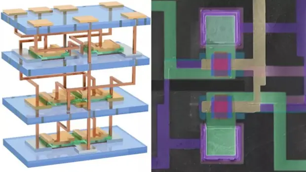
The process uses ultrathin freestanding silicon nanomembranes, just 10 nanometers thick, transferred via roll lamination at temperatures no higher than 200 degrees Celsius. Junctionless transistors eliminate the need for high-temperature doping steps, keeping the thermal budget low.
Specifications
- Device yield: 98% to 100%
- Nanomembrane thickness: 10 nanometers
- Lamination temperature: ≤200 degrees Celsius
- Number of stacked layers: 3
- Transistors per layer: 625
The team built three stacked layers, each containing 625 transistors. Output current densities matched those of conventional silicon transistors produced at much higher temperatures, and the devices outperformed monolithic devices built from alternative materials by a factor of 3 to 4.
Industry backing signals commercial potential
Industry backing comes from IBM, Intel, and TSMC, signaling potential commercial interest. The research was published in Nature.
The technology addresses a key challenge in 3D chip stacking: maintaining high yields while stacking active layers. Previous approaches often suffered from thermal damage or poor device performance. This low-temperature lamination technique preserves device quality across layers.
What is confirmed: the method achieves near-perfect yields, uses 10 nm nanomembranes, operates below 200°C, and delivers performance comparable to high-temperature silicon. Practical implications include denser, more powerful chips for computing and memory.
Source: TweakTown