NINTENDO Beast of Reincarnation Confirmed for PlayStation, Xbox, PC, and Switch GEFORCE RTX Dell Alienware 16X Aurora, Area-51 16 and 18 Launch in India PHONES iPhone 18 Pro to Feature True Variable Aperture and 2nm A20 Pro Chip PHONES Xiaomi 17 Fold and Pad 9 clear China certification, launch nears GAMES The Division 2 Update TUY8S2.2 Launches July 21 With Free Expansion Access GEFORCE RTX RTX 50 Series GDDR7 Memory Temps Now Readable Per Module NVIDIA NVIDIA Synthetic Video Detector hits 92% accuracy on AI media CONSOLES The Blood of Dawnwalker Gold Status Confirms Full Disc Release PC HARDWARE MacBook Neo Beats Lenovo IdeaPad Slim 5x in Video Editing FRAME GENERATION Winhanced 0.9.9.2 Update Fixes Handheld Power Instability GEFORCE RTX Lenovo Legion 9 18IAX10 Gets Core Ultra 9 290HX Plus for 7% Boost PLAYSTATION 5 Persona 4 Revival Confirms Chie Satonaka Voice Actors and Release Date AMD Ayaneo Next 2 Prices Surge Past $5,000 Amid Storage Cost Hikes STEAM Assassin’s Creed Odyssey Player Count Surges After Nolan Film Release

AMD Zen 7 ‘Grimlock’ CPUs to Skip Nodes, Use TSMC A14 for Late 2028 Launch

Owen Carter 0 comments 2 min read

AMD's upcoming Zen 7 Grimlock CPUs reportedly skip intermediate nodes to use TSMC's A14 process, targeting a late 2028 launch with significant IPC gains.

AMD Zen 7 Grimlock CPU architecture diagram
PC HARDWARE

's next-generation Zen 7 CPUs, codenamed Grimlock, are reportedly targeting a late 2028 launch window after skipping intermediate manufacturing nodes to adopt TSMC's A14 process technology.
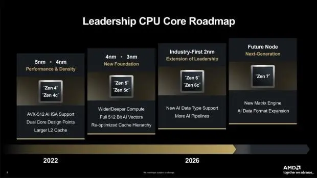
AMD Zen 7 Grimlock CPU architecture diagram

Flagship chiplet will feature up to 16 cores and next-generation cache technology

The flagship CCD architecture will feature up to 16 cores per chiplet and utilize next-generation 3D V-Cache to deliver up to 224MB of total L3 cache within a single package.

Zen 7 aims for a significant performance uplift over its predecessor, targeting a 15% to 25% IPC improvement while integrating enhanced AI acceleration capabilities directly into the CCD design.
TSMC A14 process node manufacturing facility

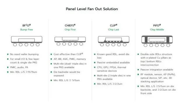
Supply chain reports indicate AMD is securing advanced FOPLP packaging allocations through visits to Powertech Technology, reducing reliance on TSMC's internal packaging operations for future chiplet assembly.

Production timelines align with TSMC Fab 25 P1 trial runs scheduled for 2027, leading into mass manufacturing in 2028 before the Zen 7 architecture reaches consumer markets.

Industry insiders suggest these architectural changes represent a major shift from AMD's previous roadmap, which previously considered intermediate nodes like N2P and N2X before committing to the 1.4nm-class A14 process.

The Grimlock CCD specifications remain unconfirmed by AMD but reflect detailed supply chain intelligence regarding next-generation CPU manufacturing processes and performance targets for the late 2028 release window.

Source: TweakTown
AMD

Discussion

0 comments

Leave a comment