Intel CEO Lip-Bu Tan confirmed that the company has started development on its future 10A and 7A fabrication processes. These next-decade technologies will eventually succeed the current 18A node and the upcoming 14A production line. Intel plans to use high numerical aperture extreme ultraviolet lithography tools for these advanced nodes.
Intel advances 14A process node with October PDK release for external partners
The company is currently advancing its 14A process, which measures approximately 1.4 nanometers. Intel expects risk production for this node in 2028 and volume manufacturing by 2029. The firm has already released version 0.5 of the process design kit for external partners to evaluate yields.
Intel aims to deliver version 0.9 of its 14A process design kit to outside customers in October. Internal teams will receive earlier access to ensure quality standards are met before commercial release. Multiple unnamed companies have already engaged with Intel regarding capacity and product definitions for the 14A node.
Tan highlighted that external partners are increasingly seeking long-term roadmap visibility alongside immediate products. The company is also preparing its EMIB advanced packaging technology, which recently achieved a 90% yield rate. Several clients have prepaid for substrates to secure supply amid tight market conditions.

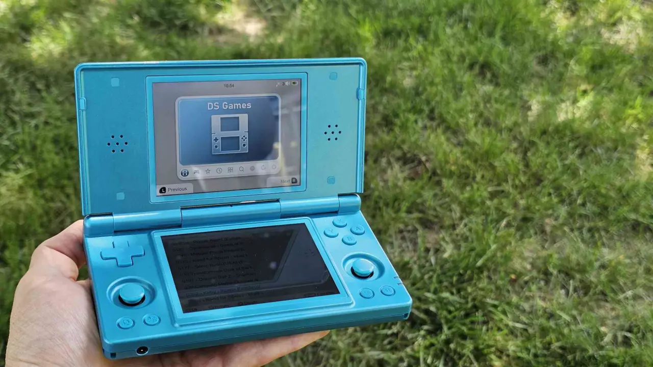
Source: Anbernic RG DS, RetroHandhelds