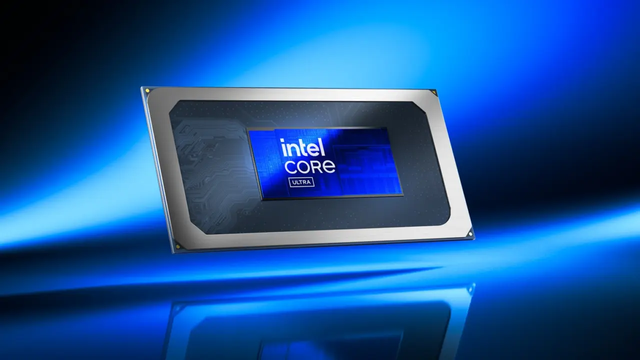
Intel’s Panther Lake processor marks a shift in how the company builds silicon, bringing two new manufacturing technologies to a consumer chip for the first time. This matters because it tests whether Intel’s internal process can compete with external foundries in a real-world product. Buyers and analysts now have independent data on how the new 18A node performs against established rivals.
Teardown reveals mixed-source GPU tiles and architectural updates
A teardown of the Core Ultra 7 365 model by SemiAnalysis reveals the internal layout of the chip. The processor uses Foveros-S packaging to combine separate compute, GPU, and I/O tiles on a passive silicon base. This modular design allows Intel to mix different manufacturing sources for different parts of the same chip.
Specifications
- Process Node (Compute Tile): Intel 18A
- Process Node (GPU Tile): Intel 3 (4-core) or TSMC N3E (12-core)
- Transistor Technology: RibbonFET (GAA)
- Power Delivery: PowerVia (Backside Power Delivery)
- CPU Core Architecture: Cougar Cove (Performance) / Darkmont LP (Efficiency)
The compute tile relies on Intel 18A, which introduces RibbonFET transistors and PowerVia backside power delivery. These are Intel’s versions of gate-all-around technology and a new power distribution method. The GPU tiles take a different path, with a four-core Xe3 unit built on Intel 3 and a larger 12-core version made by TSMC using N3E. This split sourcing highlights the complexity of transitioning to a new internal process.
Inside the CPU, the new Cougar Cove performance core fits 20% more L2 cache into a similar area compared to previous generations. Each core now holds 3 MB of L2 cache, up from 2.5 MB. The efficiency cluster uses a four-core Darkmont LP arrangement. Intel also updated its AI accelerator, with NPU 5 taking up 36.9% less area than NPU 4 while adding native FP8 support.
SemiAnalysis measured the 18A compute logic and found its density to be roughly on par with TSMC’s N3E process. The analysis notes that an Xe3 core on Intel 3 is about 55% larger than one on TSMC N3E, reflecting the maturity gap between the two nodes. While the density is competitive, the teardown suggests Intel has yet to prove a lasting edge in performance, efficiency, or manufacturing cost over TSMC. We have been tracking Panther Lake closely — see our earlier coverage on HP OmniDesk Mini.
Intel has successfully placed both RibbonFET and PowerVia into a consumer chip, according to the teardown. The hardware confirms the architectural details of the Cougar Cove and Darkmont LP cores. The mixed-source GPU strategy remains in place for the initial launch. The data provides a concrete baseline for evaluating Intel’s manufacturing progress against industry standards.
Source: Panther Lake teardown, NotebookCheck

Discussion
0 comments