FSR Onimusha: Way of the Sword Steam Deck Performance Guide NINTENDO SWITCH 2 Digimon Story: Time Stranger DLC ‘A Hero’s Eternal Legacy’ Announced PLAYSTATION 5 Cygames Launches Where the Seeds Fall for PS5, Switch 2, and PC PLAYSTATION 5 Dragon Ball Xenoverse 3 Trailer Reveals New Android Avatar Race PLAYSTATION 5 Uncanyon Puzzle Adventure Announced for PS5, Xbox Series, Switch 2, and PC NINTENDO Final Fantasy Resonance Demo Now Live With Save Carryover HANDHELD GAMING FunnyPlaying Retro Pixel MiniGB Brings Game Boy Cartridges to a 2.6-Inch Handheld CONSOLES LEGO PlayStation Set Ships October 4 for $180 With Opening Disc Drive NINTENDO SWITCH How To Fish Console Availability: PS5, Xbox Series X|S, and Switch DLSS NVIDIA DLSS Multi Frame Generation Mod Brings Blackwell Tech to RTX 40 Series GAMES Killing Floor 3 Update 2.017 Fixes Stuttering and Buffs Damage PC HARDWARE Acer EP130K ePaper Monitor: 13.3-inch 3.2K Display Ships in 2027 AYANEO MSI Claw 8 EX AI+ Gets $1,499 Price Cut With Arc B370 GPU GAMES GTA 6 Miami Marketing Blocked by Sheriff Over Crime Stereotypes

AMD Zen 7 ‘Grimlock’ CPUs to Skip Nodes, Use TSMC A14 for Late 2028 Launch

Owen Carter 2 min read

AMD's upcoming Zen 7 Grimlock CPUs reportedly skip intermediate nodes to use TSMC's A14 process, targeting a late 2028 launch with significant IPC gains.

AMD Zen 7 Grimlock CPU architecture diagram
PC HARDWARE

's next-generation Zen 7 CPUs, codenamed Grimlock, are reportedly targeting a late 2028 launch window after skipping intermediate manufacturing nodes to adopt TSMC's A14 process technology.
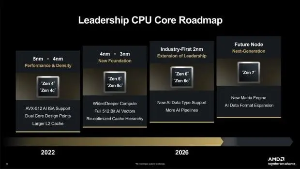
AMD Zen 7 Grimlock CPU architecture diagram

Flagship chiplet will feature up to 16 cores and next-generation cache technology

The flagship CCD architecture will feature up to 16 cores per chiplet and utilize next-generation 3D V-Cache to deliver up to 224MB of total L3 cache within a single package.

Zen 7 aims for a significant performance uplift over its predecessor, targeting a 15% to 25% IPC improvement while integrating enhanced AI acceleration capabilities directly into the CCD design.
TSMC A14 process node manufacturing facility

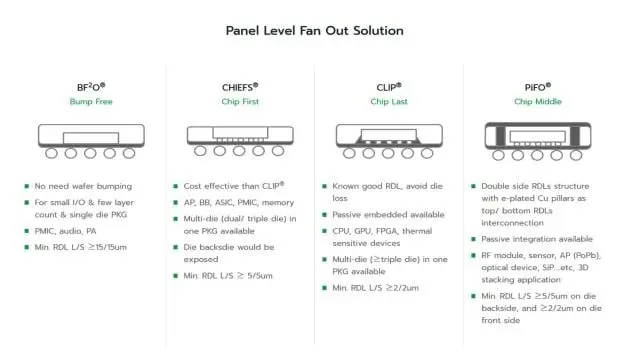
Supply chain reports indicate AMD is securing advanced FOPLP packaging allocations through visits to Powertech Technology, reducing reliance on TSMC's internal packaging operations for future chiplet assembly.

Production timelines align with TSMC Fab 25 P1 trial runs scheduled for 2027, leading into mass manufacturing in 2028 before the Zen 7 architecture reaches consumer markets.

Industry insiders suggest these architectural changes represent a major shift from AMD's previous roadmap, which previously considered intermediate nodes like N2P and N2X before committing to the 1.4nm-class A14 process.

The Grimlock CCD specifications remain unconfirmed by AMD but reflect detailed supply chain intelligence regarding next-generation CPU manufacturing processes and performance targets for the late 2028 release window.

Source: TweakTown
AMD