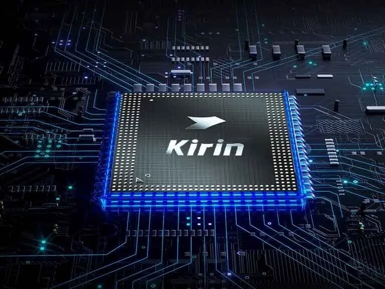
HiSilicon's new Kirin 9030 Pro processor shows that Chinese chipmakers can squeeze advanced performance from older manufacturing equipment. A teardown by SemiAnalysis reveals the chip uses a 32.5 nm metal pitch, which is tighter than Intel's upcoming 18A process. This technical achievement matters because it proves that Self-Aligned Quadruple Patterning can still push transistor density forward without relying on extreme ultraviolet lithography. Buyers interested in the future of semiconductor manufacturing should watch how this approach scales.
SemiAnalysis teardown reveals tight metal pitch and density gains from mature nodes
The system-on-chip powers Huawei's upcoming Mate 80 Pro and Mate 80 Pro Max smartphones. It integrates custom Taishan V124 CPU cores and a Maleoon 935 GPU for graphics processing. The design also includes an Ascend NPU for artificial intelligence tasks and a Balong 5G-A modem for connectivity. This configuration positions the Kirin 9030 Pro as a flagship solution for Huawei's next generation of devices.
Spec comparison
| Spec | Kirin 9030 Pro | Intel 18A | TSMC N6 |
|---|---|---|---|
| Metal Pitch | 32.5 nm | 36 nm | N/A |
| Transistor Density | 113M / sq mm | N/A | 108M / sq mm |
| CPU Architecture | Taishan V124 | N/A | N/A |
| Manufacturing Node | SMIC N+3 | Intel 18A | TSMC N6 |
SMIC manufactures the Kirin 9030 Pro on its N+3 node using deep ultraviolet lithography. The foundry relies heavily on Self-Aligned Quadruple Patterning to achieve the necessary feature sizes. The chip reaches a transistor density of 113 million transistors per square millimeter. This density figure exceeds TSMC's older N6 process, which holds 108 million transistors per square millimeter.
Performance analysis shows the Taishan architecture delivers speeds comparable to Arm's Cortex-X2 core from 2021. The chip's prime CPU core consumes approximately 4.5 watts to handle specific integer workloads. Apple's small efficiency cores outperform Huawei's highest-performance core in those same tasks while using only about one watt of power. This efficiency gap highlights the trade-offs of using mature manufacturing nodes for high-performance computing.
Huawei is pursuing architectural optimizations like LogicFolding and the Tau Scaling Law to improve performance without EUV. These methods allow the company to maximize the potential of its current hardware capabilities. The Kirin 9030 Pro serves as a practical example of how design innovations can compensate for manufacturing constraints. We looked at similar efficiency challenges earlier while tracking global semiconductor trends.
Source: NotebookCheck