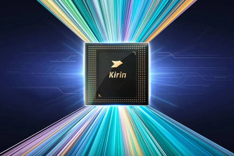
Huawei is introducing a new semiconductor design strategy called Tao Law as an alternative to traditional Moore's Law scaling. The company plans to release its first commercial product based on this architecture, the Kirin 2026 mobile chip, in autumn 2026. This approach focuses on reducing signal delay and increasing transistor density through a method known as logic folding.
Logic folding technique aims for higher density without scaling
The Tao Law strategy shifts away from geometric transistor scaling by shrinking time delays within circuits. Huawei states that this technique allows for higher transistor density across devices, chips, and systems without relying on traditional manufacturing advances. He Tingbo, president of the company's semiconductor business division, noted that engineers have designed and mass-produced 381 chips using this method over a six-year period.
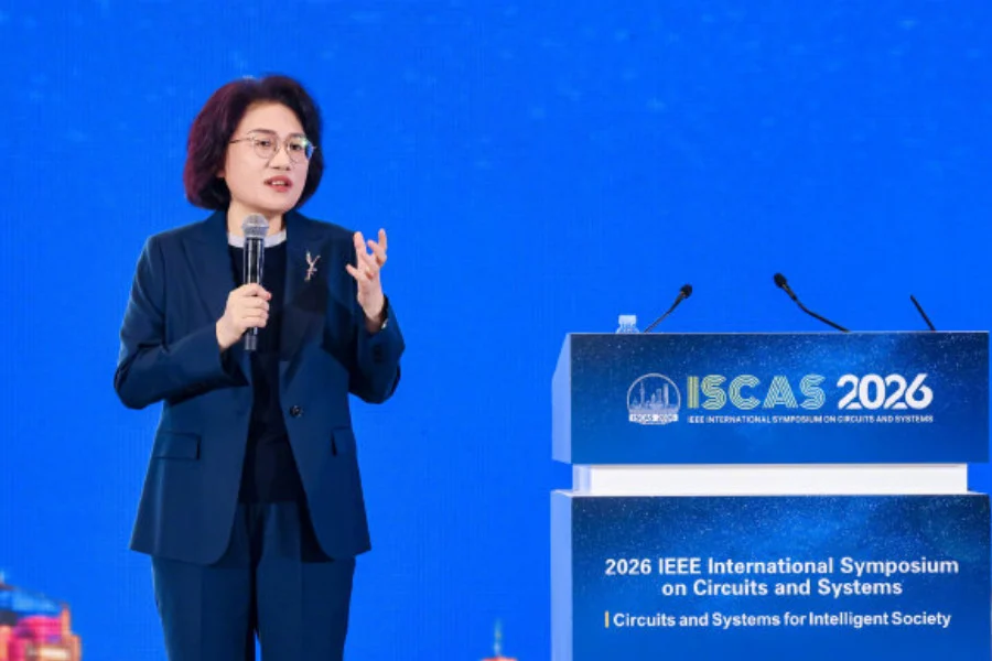
According to internal claims, the architecture could eventually match the performance levels of future 1.4nm processors by 2031. The company asserts that Tao Law will significantly improve both performance and energy efficiency across its hardware lineup. Industry observers note that these projections rely on a new architectural approach rather than conventional process node improvements.
The announcement positions Huawei's latest chip development within the broader semiconductor industry landscape. The strategy offers a potential pathway for manufacturers to continue improving hardware capabilities without depending solely on advanced fabrication techniques.
Source: GIZMOCHINA