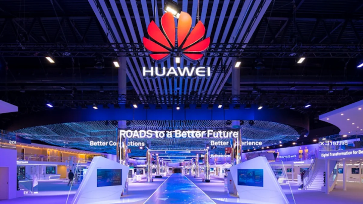
Huawei unveiled a roadmap for advanced semiconductor manufacturing that aims to bypass U.S. sanctions by developing domestic alternatives to ASML's EUV lithography machines. The company plans to launch a process equivalent to TSMC's 1.4nm node by 2031 using its new LogicFolding Design architecture.
He Tingbo presents advanced EUV bypass strategy at IEEE conference
He Tingbo, President of Huawei's Semiconductor Business Unit, presented the technology at IEEE ISCAS 2026 in Shanghai. Next-generation Kirin mobile processors will be the first commercial chips to feature this logic folding approach.
The LogicFolding approach adjusts the arrangement of transistors to shorten signal paths and enhance speed while maintaining existing physical sizes. This technique enables the company to reach comparable performance levels by refining chip architecture and assembly instead of depending on outside manufacturing equipment.
Huawei is investing in domestic suppliers like SiCarrier to build EUV machinery required for the roadmap. Reports suggest Huawei may have participated in a high-possibility funding round for SiCarrier, though this has not been confirmed.
The company's strategy focuses on self-reliance amid ongoing restrictions. Through the development of domestic design and production skills, the company seeks to maintain its device product lines independently of international supply chains.
Source: GIZMOCHINA